-
 JP22
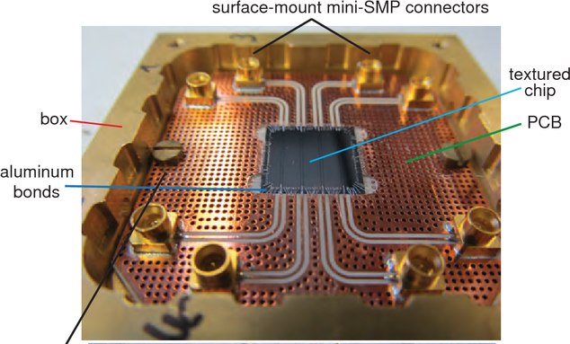
0I am designing a PCB to interface with a smaller chip that has CPW-based RF circuits operating at 5-10 GHz. The PCB will have SMP connectors at the edge, with CPWs routed to the center where they will be wire bonded to the CPWs on the chip. It is a single layer PCB with a metal-plated backplane. I have attached an example image.
JP22
0I am designing a PCB to interface with a smaller chip that has CPW-based RF circuits operating at 5-10 GHz. The PCB will have SMP connectors at the edge, with CPWs routed to the center where they will be wire bonded to the CPWs on the chip. It is a single layer PCB with a metal-plated backplane. I have attached an example image.
In my field of research, it is common practice to add a grid of vias connecting the ground planes on the top layer with the backplane. This has two main purposes: 1 - These are devices that operate at cryogenic temperatures, and we need a thermal connection between the top layer of the PCB and the backplane, which is mounted on the cold metal finger; 2 - We want to supress unwanted resonance modes from the larger volume of dielectric that constitutes the PCB.
My RF intuition says that we want to avoid vias as much as possible because of the extra inductance, so when I see these grids of vias on CPWs I cringe a bit. I'm trying to design my own PCB, and I was wondering if this practice of adding grids of vias to supress unwanted modes is common, and whether anyone knows any references to help me design this more effectively. I have a feeling that I can get away with a much lesser dense grid than show in the picture, but I'm not sure how to design it.Attachment 29-Figure3.4-1
(743K)
29-Figure3.4-1
(743K)


Welcome!
Join the international conversation on a broad range of microwave and RF topics. Learn about the latest developments in our industry, post questions for your peers to answer, and weigh in with some answers if you can!
Categories
- About Our Site
- Antennas
- Applications
- Biological Effects and Applications
- Calculators
- Communications
- Computer Aided Design
- EDA Software
- Emerging Applications and Technology
- Employment
- Field Theory
- Filters and Passives
- General Questions
- High Power
- History
- MMIC and RFIC
- Packaging and Materials
- Radar
- Sources and Receivers
- Test and Measurement
More Discussions
- Terms of Service
- Useful Hints and Tips
- Sign In
- © 2026 Microwaves 101 Discussion Board